
Last June, we announced SOSV’s latest deep tech expansion, the HAX Plasma Forge, a program launchpad dedicated to founders turning breakthroughs in plasma science into real-world companies and a space for corporates to access cutting-edge R&D co-located with innovators. HAX Plasma Forge will harness the latest advancements in plasma applications to build the critical infrastructure behind AI, with a focus on companies in the Advanced Computing, Energy, and Manufacturing industries.
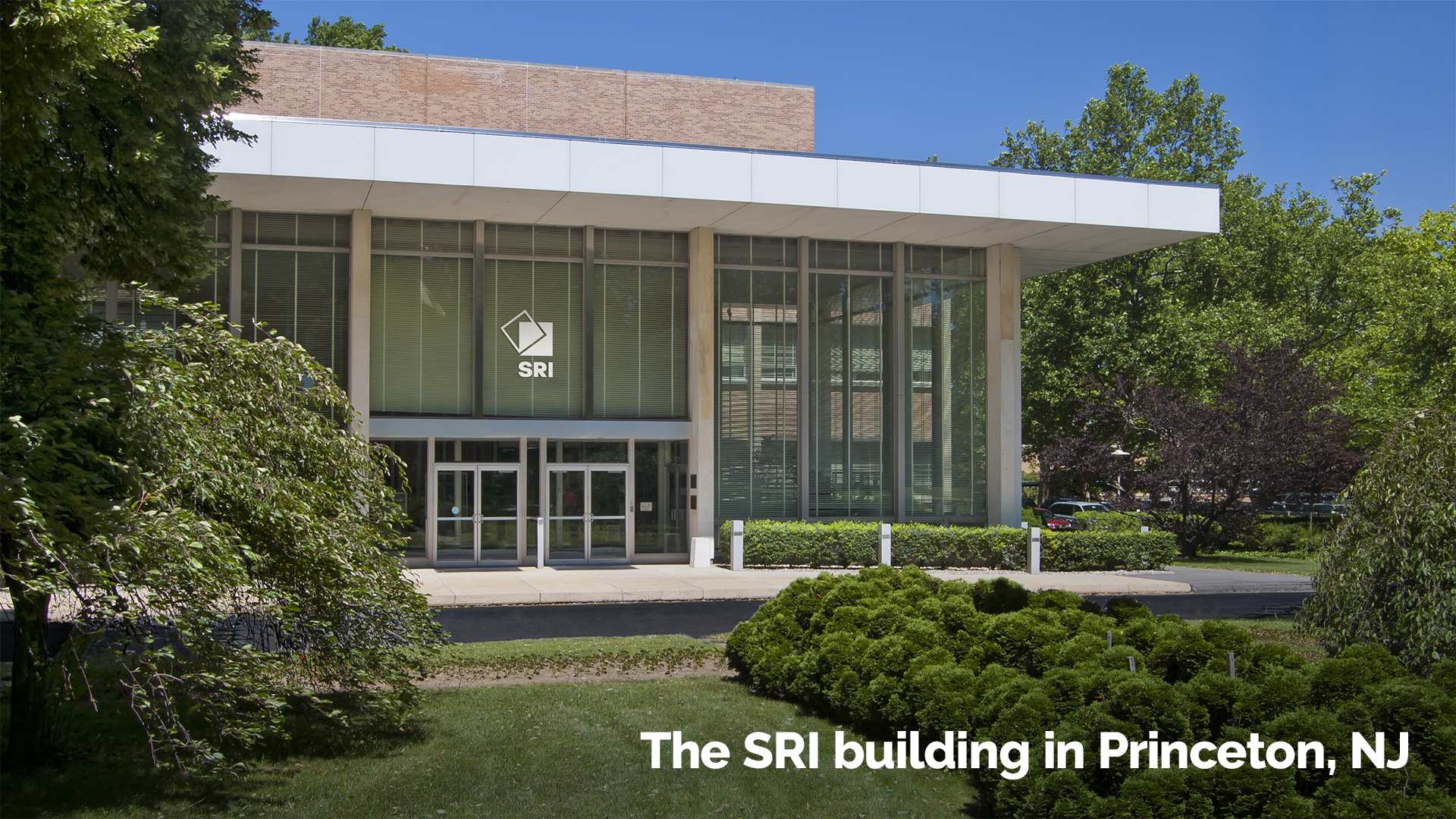
Today, we’re excited to announce that HAX Plasma Forge will be headquartered in Princeton, N.J. at SRI, one of the most storied innovation centers in U.S. history.
The HAX Plasma Forge isn’t just renting space, they’re joining a lineage of innovators who specialize in turning frontier science into the bedrock of global industry.

SRI, located at 201 Washington Road, in Princeton, N.J. isn’t just a building; it’s a quiet engine where technologists worked on many technologies key to the modern world. Formerly RCA Laboratories and the David Sarnoff Research Center, these halls are where foundational technologies including color television, LCD displays, and early semiconductor innovations were born. During World War II, breakthroughs and development at this site contributed to radar and defense systems. In the decades since, it has continued to push the boundaries of imaging, sensors, advanced materials, and more.
“The HAX Plasma Forge isn’t just renting space, they’re joining a lineage of innovators who specialize in turning frontier science into the bedrock of global industry,” said David Parekh, CEO of SRI. “We can’t wait to see plasma become the next great chapter in that legacy.”
The Plasma Forge Model
At SOSV HAX, we’ve spent years in the trenches with founders, helping them to turn deeply technical ideas and research into commercialized products. The HAX Plasma Forge is an extension of that model, combining:
- A Commercialization Engine: Founders gain access to HAX’s proven program model for hard tech growth, turning “bench science” into investable, scalable companies.
- An Elite Scientific Alliance: Through our partnership and proximity to the U.S. Department of Energy’s Princeton Plasma Physics Laboratory (PPPL), who are world leaders in advances in plasma physics research and development, plasma metrology, and advanced plasma modeling, founders tap into a level of expertise and specialized resources that are rarely found outside research labs.
- Sustained Institutional Backing: With $51 million in dedicated funding, including $24.5 million from SOSV, $24.5 million over the course of a five-year partnership from the New Jersey Economic Development Authority (NJEDA), and additional technical collaboration and in-kind support from PPPL, we have the financial runway needed to scale ongoing operations.
- A Robust Ecosystem: By co-locating early-stage plasma startups with corporates and other innovators using plasma, we’re fostering an environment to promote innovation and application of plasma physics.
When the doors open in late 2026, founders will have access to 10,000 square feet of purpose-built and expansive long-term lab and working space, including:
- Up to $550K in Seed capital from SOSV
- Access to specialized plasma R&D infrastructure and metrology
- Hands-on support from SOSV HAX’s engineering, design, and supply chain teams
- Co-location with corporates looking to better understand and adopt plasma technologies
- Direct collaboration with world-leading plasma scientists from PPPL
- Connection to SOSV’s global network of founders, investors, and partners
As we get closer to launch, we are also proud to have assembled an all-star HAX Plasma Forge Advisory Board, bringing together some of the most respected names in the field. This group will play a hands-on role in evaluating incoming startups, validating their technologies’ fit with market needs, supporting founders as they navigate technical and commercialization challenges, and helping shape the strategic direction of the HAX Plasma Forge.
- Dr. Richard Gottscho: Former CTO & EVP Global Products at Lam Research; World leader in plasma processing for semiconductor manufacturing
- Dr. Gilroy Vandentop: Head of Industry Partnerships at Texas A&M Semiconductor Institute, Former Engineering Manager and VP of Corporate University Research at Intel, selected to play leadership role at Semiconductor Research Corporation; Leader in plasma technologies
- Dr. Kieran Drain: Former Managing Director at Applied Materials and CEO of Tyndall Institute; Veteran executive with leadership experience at both research institutes and industry; Operator with expertise translating advanced materials into scalable businesses
- Faran Nouri: Former Sr. Partner Natcast, Vice President at Lam Research & Global Head of Lam Capital, and Director at Applied Materials; Semiconductor technologist, entrepreneur, and venture investor with over three decades of leadership spanning product development, corporate strategy, venture capital, and M&A
- Dr. Chantal Badre: Deputy COO & Chief of Staff at PPPL; Strategic and Operational leader at PPPL, bringing deep expertise in translating science into scalable industry impact, with prior global leadership experience in strategy, business development and innovation across markets in the chemical industry
- Dr. Ahmed Diallo: Distinguished Research Fellow at PPPL; Plasma physics expert, Currently leading PPPL efforts on enabling technologies for energy and science, and is a former Program Director at ARPA-E
- Dr. Yevgeny Raitses: Distinguished Research Fellow at PPPL; Expert in fundamental science of plasma technology for materials synthesis, advanced semiconductors and space propulsion
Why Plasma?
People often ask, “Why the focus on plasma?” It’s a fair question. Plasma has been “the future” for a long time. But we believe we’ve reached a massive inflection point for two specific reasons:
First: AI is reshaping the physical world.
The rapid acceleration of AI is reshaping where value accrues in technology. As software gets cheaper and more abundant, the bottlenecks are shifting to infrastructure: energy, compute, materials, and manufacturing. Meeting this demand requires breakthroughs in clean power, semiconductors, and electrified, resilient industrial systems – plasma sits at the center of all three.
Nowhere is this more evident than in semiconductor manufacturing. Plasma-based processes already represent 45% of the 400-950 process steps in manufacturing leading-edge chips, meaning virtually every chip in circulation today has been shaped by plasma. As AI drives exponential demand for faster, more efficient, and lower-cost compute, plasma is being pushed to do even more. At the same time, advances in fusion – long considered decades away – are accelerating, with leaders increasingly expecting fusion power to reach the grid in the 2030s, further reinforcing plasma’s central role in powering the next generation of intelligent infrastructure.
Plasma physics was invented in the 1950s when we weren’t as far along as normal chemistry, but in the last two decades plasma physics has got up to speed in its predictive capability.

Second: AI is making plasma controllable.
For decades, plasma systems were notoriously difficult to predict and to manage – dynamic, nonlinear, and evolving faster than human operators could respond. Today, AI-driven control systems are changing that. We can now tune and stabilize plasma processes in real time, enabling reliable operation in industrial environment.
“Plasma physics was invented in the 1950s when we weren’t as far along as normal chemistry, but in the last two decades plasma physics has got up to speed in its predictive capability,” said Sir Steve Cowley, Director at PPPL, at a recent SOSV Deep Tech Live event. “The industries surrounding it are suddenly getting this injection of capability that we didn’t see before — where we were largely doing Victorian-type engineering, we’re now carefully putting a single monolayer of atoms down in order to make some particular device. It’s exquisite in the way that you can now manipulate at the scale of atoms.”
This changes everything. For the first time, plasma is not just scientifically powerful, it is commercially actionable, and the expertise at PPPL is a key unlock to harnessing plasma for transformative applications.
The Future is Electrified. Come Build It With Us.
➡️ If you’re a founder: We’re looking for the most promising companies spanning plasma and plasma enabling technologies, semiconductor fabrication, advanced materials, and manufacturing: Apply to the HAX Plasma Forge today.
➡️ If you’re a corporate: We’re looking for companies utilizing plasma technology in their products and looking to get better connected to the innovation ecosystem to co-locate at the HAX Plasma Forge. Contact via this form on SOSV.
➡️ If you’re an operator who loves to sit at the interface of scientific innovation and commercialization: We’re hiring a Site Manager to help build and run the HAX Plasma Forge, owning day-to-day operations, lab maintenance and safety, serving as part of HAX’s investment team, working 1:1 with founders, and more: Find more info on the role and apply to be the HAX Plasma Forge Site Manager today.
New Jersey’s Strategic Innovation Centers (SICs)
The HAX Plasma Forge was previously announced as part of the state’s Strategic Innovation Center (SIC) initiative. SICs are facilities that support research and development, innovation, and entrepreneurship through mentorship, networking opportunities, hands-on training, business support services, and education opportunities. New Jersey has announced 12 SICs across the state, collectively projected to create $8.9 billion in direct economic impact and support 28,000 jobs by year 10 of operation.